Atari 1040STFM Restoration 👨🔧

For everyone in IT there is this one single bike one learned riding on. Albeit my first experiences with computers reach back to a Sinclair ZX81 and its Sinclair BASIC at the age of six, it took another three years to get a proper home computer.
Whatever arguments one put up as justification getting a home computer, we all know it has been all about gaming.
Looking back it turns out that making this decision for the financial sponsors has been pretty hard. Commodore, Amiga, Atari and a couple of others fought the home computer war and evaluation of needs versus capabilities hasn't been as easy as it is nowadays. Especially without computing background, market overview and false advertising the choice could most probably be no good. Frankly, the choice most likely reflected the character of the buyer rather than the user.
Even today when meeting IT people with a history routed in the late 80's or early 90's, after some nostalgic talk there is a fair chance one could guess the others first home computer 😁
Retr-O-Spective
Being replaced by a Toshiba Satellite Laptop (Intel 486 DX4 afair) somewhere around 1994 or 1995 this Atari has probably never been woken up since the mid nineties. By the time of writing this is 26 years of hibernation.
First Impressions
A first glimpse shows the typical patina one would expect. The lid of the Floppy Disk Drive (FDD) is missing (not sure if it ever had one though 🤷♂️).

Apparently there is no hint pointing to a major issue.
Lab Setup
Without the usual peripherals (a mouse and a monitor should do) powering the Atari up wouldn't make great sense. Unfortunately the mouse misses its ball and the cable isn't in its best condition but for connectivity this should do. I do still have the high resolution monochrome monitor (SM124) which does not seem to have major damages as well.
As a backup a simple usb video capture USB stick will do to capture the video signal.
For the electrical analysis I use a Rigol DS1104Z oscilloscope, a Rigol DL3021 DC Load, a Rigol DP832 Power Supply and a Mastech MS2115B Multimeter.
Teardown and Cleanup
The overall condition is not too bad. It seems this machine has undergone a repair already. What makes me wonder is I always owned an STFM and the shell does only shows the STF label. I somewhat recall it got another shell after repair since the disk drive has been changed to a disk drive with the long trapezoid eject button but this is many years ago so I can't really tell.
Let's have a look at the insides and identify the model: The main board is a C103414-001 REV 1.1. This seems to be correct for an STF/STFM, but per this link https://temlib.org/AtariForumWiki/index.php/Atari_ST_motherboard_revisions it matches a 520.
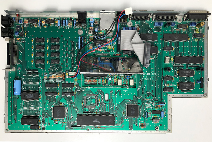
Let's check the RAM. It has 8 x OKI M514256 build in. Each one holds 262.144 4-bit words which give 128K ram per chip. Overall those are 1.024K or 1M of ram.
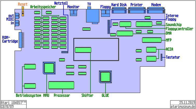
Also it clearly has the Television port so it actually is an STFM! Hooray 🎉🎉🎉! atarimuseum.de has a pleasant drawing of the layout (note there are some differences since this is C070789). I'll leave the spotting of parts to you.
General Specs
TOS
C101635-001 = TOS 1.02 2Chip Deutschland High
C101636-001 = TOS 1.02 2Chip Deutschland Low
Power Supply Unit (PSU) Check, Part 1
I try to follow a proper functionality check path and investigate the PSU first. It is a Mitsumi SR98 (Schematics).
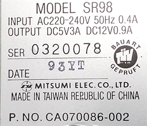
For most parts the schematics and specs can be found online. The electrical characteristics for the PSU are:
| Input Voltage | AC220V |
| Input Voltage Range | +/- 10% |
| Frequency | 50 Hz |
| Rated Current | 2A max. |
| Inrush Current | 35A max. |
| Output Voltage A | DC +5.1V |
| Output Current A | 1.5 - 3.0A |
| Output Effect A | +/- 0.255V |
| Ripple and Noise A | 100mV P-P |
| Start-up time A | 150msec max. |
| Hold-up time A | 10msec max. |
| Output Voltage B | DC +12V |
| Output Current B | 0 - 0.9A |
| Output Effect B | +/- 1.2V |
| Ripple and Noise B | 150mV P-P |
| Start-up time B | 150msec max. |
| Hold-up time B | 10msec max. |
| Efficiency | 55% min. |
| Withstand Voltage | AC1.25KV imin. |
| Insulation Resistance | 10MO min., DC500V |
Let's hook a DC load to it and see how it performs - if there is any performance at all ⚡️ - and if it still is in specs. I'd assume some deviance after all those years (https://www.exxoshost.co.uk/atari/last/psu/index.htm).
Disclaimer: mains voltage can kill! I'm not taking any responsibility or liability if you hurt yourself, other people or your surroundings by following this teardown!
External Power Support
Having the PSU in bad condition I decided to blow up the +5V rail first 😁. Per schematics it just needs the +5V in order to boot. I'm using the Rigol DP832 with +5V and 2.3A with an OVP of +5.1V and an OCP of 3A. Powering up the power supply the board draws 5V and approx. 1.2A. Some ICs are getting a bit warmer than room temperature so I assume something is going on.
Unfortunately I'm not holding a PhD in Electrical Engineering and logic courses during my studies is a history long gone, so I expect this to be a tougher job.
What to troubleshoot next? We all know the clock is the heart of everything digital so let's see how this behaves. The Atari uses a crystal in favour to an oscillator. You can learn about the difference here https://www.sitime.com/company/news/blog/do-you-know-when-use-crystal-or-oscillator-wrong-answer-can-cost-you.
I'm lending the picture from their side:
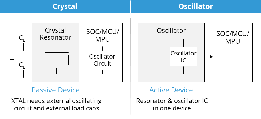
The Atari STFM uses 3 Crystals (XTAL):
- Y1: 2.4567MHz,
- Y2: 32.084988 MHz,
- Y3: 4.433618 MHz (the FM Version PAL, Y3 for NTSC is @3.579545 MHz).
Let's find where clock frequencies are generated and consumed:
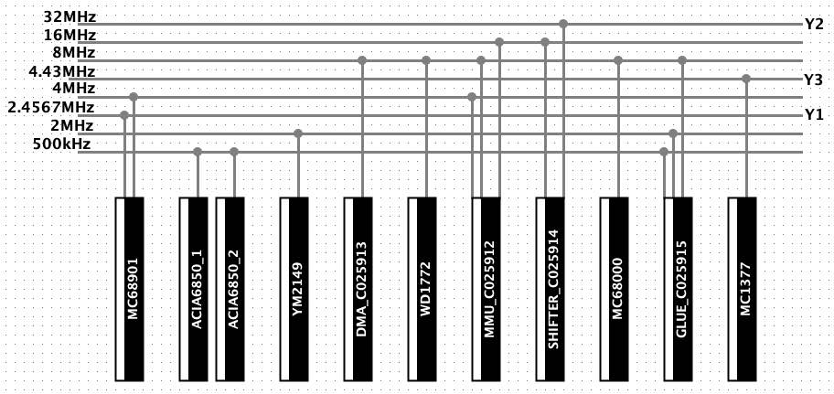
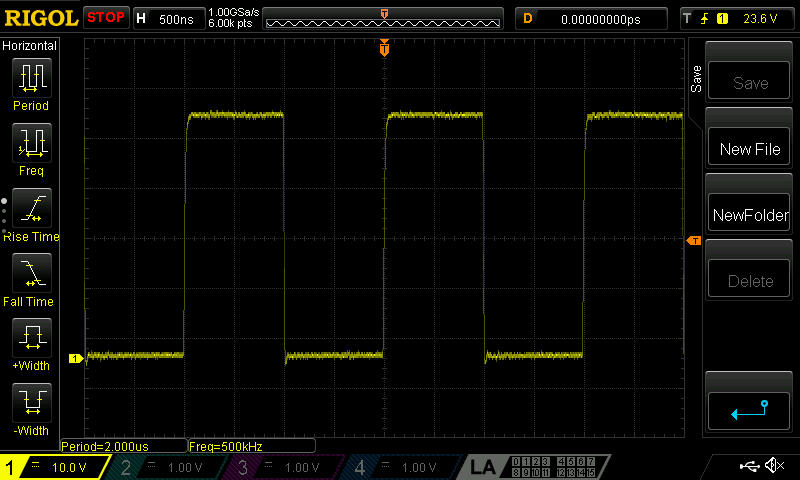
Looks like the SHIFTER (C025914) resonates the clock with the highest frequency (32MHz) and outputs a 16MHz frequency. The MMU (C025912) consumes this frequency and provides both a 8MHz and a 4MHz domain.The GLUE (C025915) takes the 8MHz and provides both 2MHz and 500kHz.
From the schematics it looks like the MC68901 is the driver for Y1 XTAL but has a 4MHz input as well. Not sure what that means but we might find out sooner or later.
That's theory now let's check all the clocks on the various ICs starting with the SHIFTER. 32MHz in:

...and 16MHz out:

The MMU takes the 16MHz:
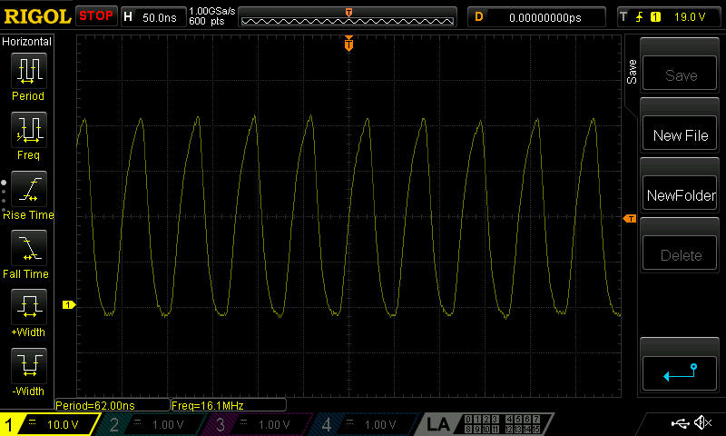
and provides 8MHz

... and 4MHz:

The MC68000 should get a nice 8MHz input clock:
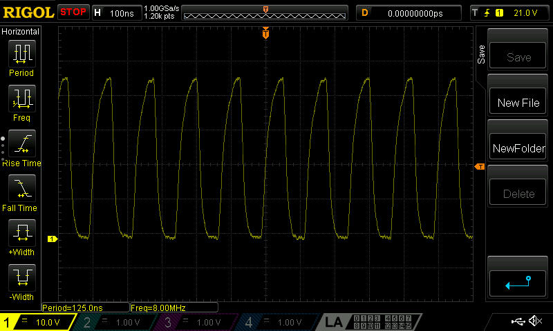
So should the DMA Controller...

...and the WD1772:
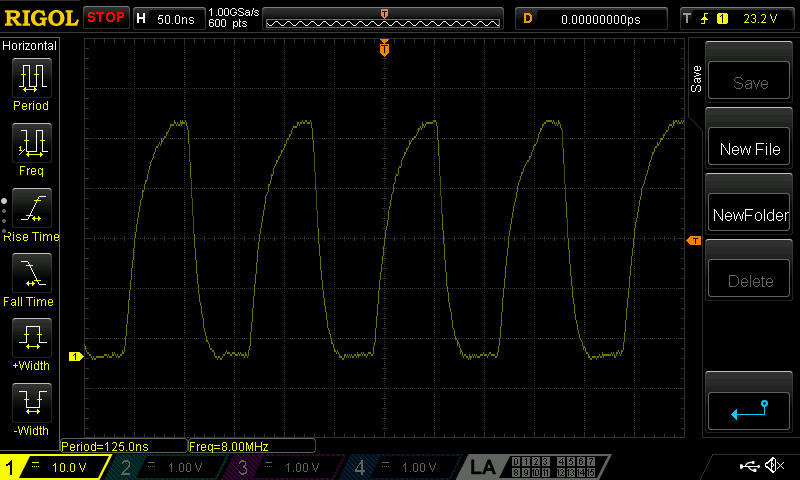
The GLUE takes 8MHz

...and provides 2MHz
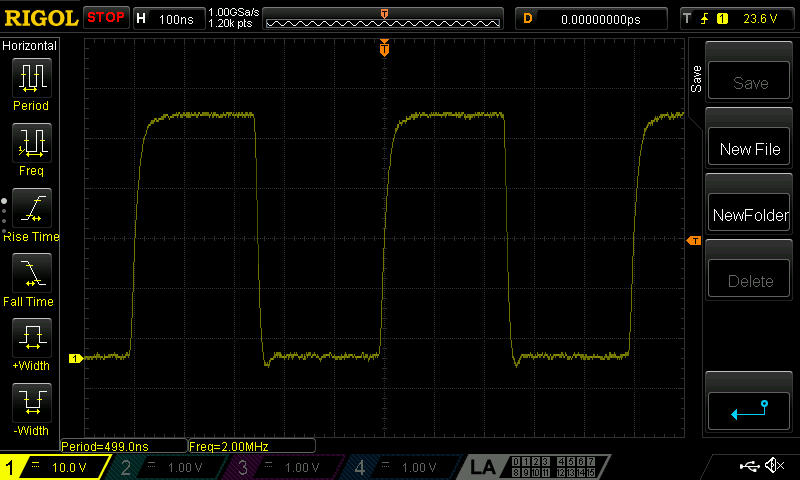
and 500kHz
The MC68901 gets 4MHz in:
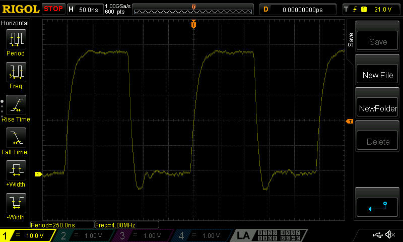
The YM2149 gets 2MHz in:
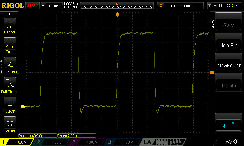
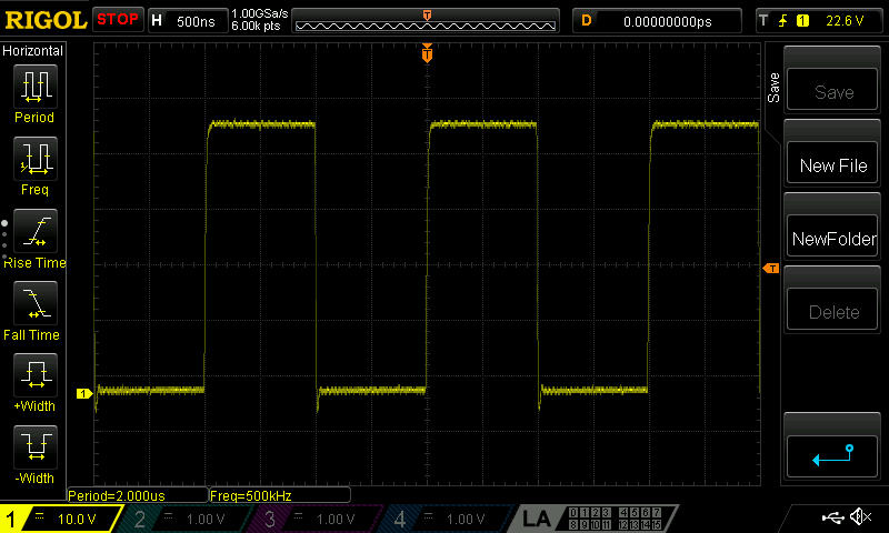
The two ACIA6850 both get 500kHz in:

Finally the MC1377 (https://forum.atari-home.de/index.php?topic=749.20) resonates Y3 and this looks good as well:
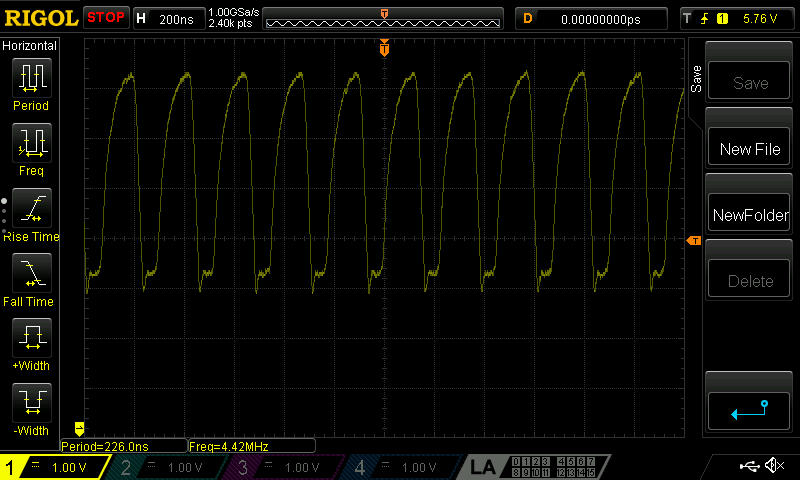
Apologies for bad voltage units but I forgot to set the probe ratio to the correct level. Since we are talking about TTL you might scale the value for your purposes accordingly 😁🙄.
Startup with 'Television' connected.... no cigar 🤨
HSYNC (pin 37 on GLUE) and VSYNC (pin 38 on GLUE) deliver 15.6kHz and 50Hz. That does sound absolutely as intended.
MMU (pin 51, VSYNC) measures 50Hz as well. Good news!
Having a look at the RGB output of the SHIFTER (pins 21 - 20) it looks like a proper output is generated. the DE line (pin 37) is roughly showing a unique 15.7kHz signal, generated by GLUE (pin39).
My S-Video to USB capture stick does not show any output 🧐...
SILLY ME! The output is RF and not S-Video. Not to blame the converter!
Probing on the 3 red outputs (D0, D1, D2) of the SHIFTER, triggered to VSYNC show that there is output but each picture consists of RED being always high for all 313 lines (please note: this is no pixel per pixel but a travel cathode ray signal). The three red TTL signales are converted to 8 analog voltage levels, like 3-bit to analog. The R-line is always 0x07. With every bit 'on' this is the highest value for red. Without measuring I expect this to be true for green and blue as well thus having a white screen.
In the picture CH1 (yellow, VSYNC) goes low on every vertical sync (50Hz, yay 🎉) and BLANK (D3) looks like everything is coming along as expected.
BLANK signal explanation (source):
The Blank signal forces the  RGB colour outputs to zero  just before,  during, and just after the Hsync and Vsync synchronization signals.  Indeed,  monitors
 require the video signal  to be 0 volts  (black colour) before  every synchronization pulse (implemented as a negative voltage): Even the border colour has to be eliminated to prevent overlaying the border colour over the screen while the electron beam returns to the beginning of the next line (from the screen's right to its left)  and to the next picture  (from the screen's bottom  to its top).  Note that the Blank signal isn't used if the screen is displaying high-resolution.
Those are my assumptions so far 🤷♂️
A quick probe on the TOS ROM ICs shows there is some data flowing out, so I'm not expecting the ROMs to be dead.
So there is nothing broken in the first place. During the last days I let the SM124 Monitor acclimatise to the climate in my room. Switching it on for a couple of minutes every other day to get the caps regenerating seemed to do the job.
Apparently DIN13 monitor plug provides composite video on pin 2 and it really does. Let's get down to the SM124.
SM124 to the rescue
It didn't im- or explode when turning it on and the oh-so-nice 'plop' sound when the speaker gets power 😁. The brightness and contrast controls are a bit wiggly.
It'a alive!
Since the 12V rail is not on external power support yet I cannot boot from a floppy disc. Turning the external power supply creates a white screen on the SM124 and then.... TOS! 🎉🎉🎉
There it is, good old TOS, mother of my GUI experiences! There is just a slight horizontal displacement of the screen but not bad enough to risk opening the monitor shell.
Power to the Floppy
My lab power supply offers 3 separate channels so there is room enough to risk powering the FDD as well. When turning it on the head tries to move back to track 00. It seems to be stuck there and moving back and forth. Maybe there is to much friction for the sled where it moves along the two guidance bars. Or maybe the stepper motor is bad. The latter wouldn't be too good, as opening it might result in painful disk alignment. As the FDD is my only chance to get data (programs!) to the ST that would be no good.
In theory one could check the Track 00 signal between FDD and FDC (floppy disk controller) in order to see if the drive does not send the signal or the FDC is in bad condition.
Cleaning the drive, greasing the rails and move it back and forth manually should do the trick. While being open I can confirm the two reed switches close to the lid are still working.
The drive is a Chinon F-354 Rev B so there is no belt we have to worry about.
Second try: no luck. It still seeks for track 00. 😒
What else...? Well there are some caps but they look good. What catches my eye is a miserably bent transistor:
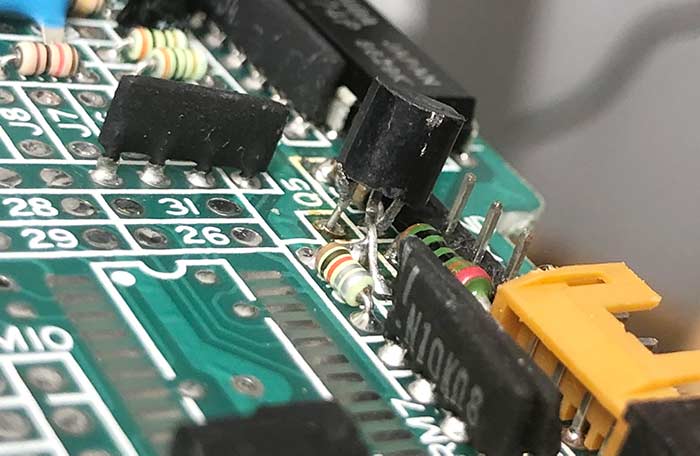
So off it goes! It is a BC 558C PNP transistor so I might have to order one first. Maybe this can be fixed otherwise. Measuring it's connections it turns out it actually is connected to the track 00 sensor (Omron Japan H30) so it might cause some troubles there. Btw. if you happen to know how the Omron thing works, let me know! I cannot find anything on the interwebs. I assume it is a hall sensor...
After de-soldering the transistor, straighten the pins, measuring it (it is in good condition at 5MOhms between base and emitter/collector) I decided to put it back in. Voilà! No more forth and back in the search for track 00! I'm still not sure if the bent transistor has been the root cause or just a poorly connected FDD cable.
Using one of the old disks shows: it actually can read those old disks coming from the attic! 🙈👏 And most of them are still good!
A couple of tests bring back some fond memories!
Replacement PSU
No matter of the condition of the built in power supply unit I decided to go for a new one neatly fitting the designated place. Thanks to centuriontech.eu I found a superb replacement.
After a couple of weeks it finally arrived. Checks on the DC Electronic Load show condition is excellent so in it goes. The main power chords need to be capped and the wires re-tinned to fit into the (blue) socket but that's no big deal I'd say.
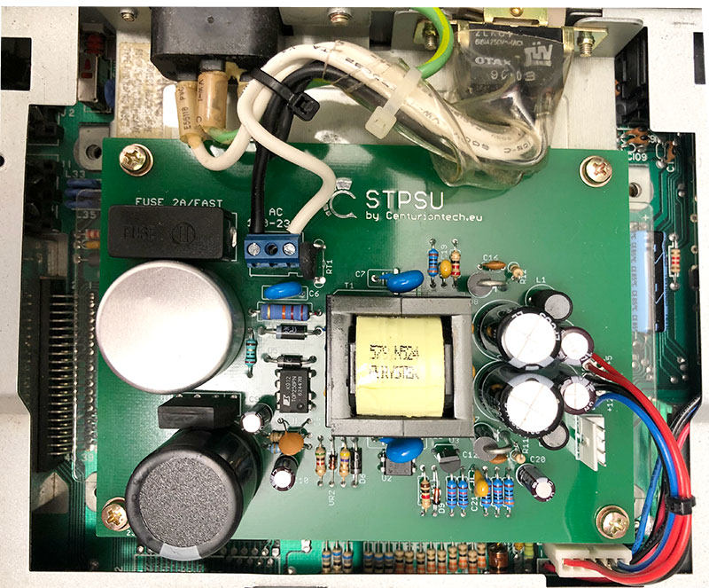
Works like a charm! 🐝🐝🐝
Preservation and Archiving
I never really wasted thoughts on the historical value of data and intellectual property in our fast evolving digital age. The topic kicked in when emotions overwhelmed when my first ever self-made computer game has been found on a floppy: Aeroescape v01! 🎮
Must've been created at the age of 11. I still wasn't to sure if this came from my hands but the later to be found source code shows exactly my handwriting 😒
I totally forgot about that and without finding it, I could never feel with all the commercial and personal efforts people put into computer games and applications.
There is a lot of good documentation about preserving old discs (for the ST here). I really did not want to mingle with floppy drive control and A/D converters (again!) it was time to get a proper device with some good software (Windows Executable, Python). There are some to choose from but I found the GreaseWeazle V4 being a good choice. It captures floppy disc on a flux level without interpretation of data. Other tools can take this low level signal stream and convert it to disk images (like ST, STX, ...). I found Aufit doing a good job. Many emulators like Hatari and Steem SSE natively ready this low level (SDC) format already.
I might post an update on this topic later on as dumping the floppy discs is till work in progress...
Video Output: Mono vs. Color
At this point I decided to give a second try to the color display (aka USB video capture device) by taking the composite video from the 13 pin monitor jack (see https://www.exxoshost.co.uk/forum/viewtopic.php?t=94). The output looks not too bad but the capture device still shows... nothing.
Seems there is some more research to be done in order to understand how this works. Sticking to this page https://info-coach.fr/atari/hardware/video.php#video_composite it cleary shows, that the signal frequency is too low to get captured by nowadays devices. I really do not want to get a multi sync monitor (like a NEC from the days) and convert the 13 pin monitor jack signal to VGA.
Apparently the Sinclair will need to be revised as well, so a RF-to-nowadays-video is a must. At this point my little DE0 Nano FPGA is catching my eye. Why not using it's analog-to-digital converters, capture the RGB, BLANK, VSYNC and HSYNC output and generate a clean VGA signal? 🙈
Apart from an easy hack is to bring the monochrome output (35.7 kHz HSYNC, 71.2Hz VSYNC) to a VGA display I really want a digital video output for modern display. Since the frequencies are in a range typical VGA displays understand, this is just a matter of wiring things up.
Video Converter
The DE0 Nano comes with a NS ADC128S022 8-Channel, 12-bit A/D Converter. It does support up to 8 input signals. Those can range between 0V and 5.25V and with a maximum of 10mA.
We want to sample 6 channels: Red, Green, Blue, BLANK, VSYNC and HSYNC. For this IC the maximum sampling rate is:
F(s) = F(SCLK) / 16 x CHANNEL.
SCLK is the digital clock input which controls the conversion and readout process. It may vary between 0.8 MHz and 3.2 MHz.
That'll make a sample rate per channel of 34 ksps per channel. In order to avoid anti-aliasing we need to meet the Nyquist criterion BW(signal)<F(s)/2. Thus we can handle 16 ksps which approx. 16kHz per channel.
VSYNC is 50Hz (PAL) so the signal is perfectly within range of an analog input signal. HSYNC is 15.6 kHz so this is all we need for this signal.
The Atari outputs the following video signal specs:
- 640 x 400 pixels, monochrome,
- 640 × 200 pixels, 4 colours,
- 320 × 200 pixels, 16 colours.
Where as it has (for PAL, 50Hz):
- 313 lines per frame,
- 512 cycles per scan line.
This means there is actually an invisible border around the 320x200 visible area. And with that, numbers do add up: 15.65 kHz on the HSYNC (50 frames per second x 313 lines per frame).
If we where to capture 320 (columns, X) x 200 (rows, Y) pixels we need to capture 320 voltage samples with one HSYNC of 15.6 kHz, thus we need 4.992 msps on each channel. This is far beyond what the A/C converter is capable of.
If we check one line on the oscilloscope we gain a better understanding of the signal. We ignore the white lines and get to the first line actually containing white and black pixels (marked in red).
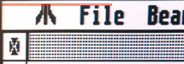
The two vertical lines mark beginning and end of this screen line (between two HSYNC, blue). Red marks our spot of interest - the only black pixels in that line.
![]()
Zooming in we expect long whites followed by black, white, black, black, white, black and long whites again:
![]()
Not too bad, exactly what we expected 😁😒
However we need some time to think about the right timings: a line is 640 pixels. HSYNC is 35.7kHz which makes one line taking 28us.
...for monochrome
If the whole payload of a line is mapped to 640 pixels we end up with approx 44ns per pixel. Our measurements show, that we only use approx 20us for the line itself. So 8us are front and back porch, probably for some housekeeping of the signal. Dividing 20us by 640 we get 31.25ns per pixel. This is pretty close to our measurements. On the other hand this means our signal could cary 28us divided by 31.25 ns/per pixel = 896 pixels.
The question is: how do we sample the analog signal? Since this is a 1 bit signal, let's try with a simple clock calculation:
There is a 1/35.700 period where we need to capture a whole line which makes our 28us.
The VSYNC (71.2Hz since this is the monochrome output) gives us 14.0440us (0.014 seconds) to capture all the lines. This would be a max of 501 lines per 'frame'.
Capturing 71.2 (Hz) times 501 (lines) times 896 (pixels) per second asks us for 31.512.499 bits so our clock needs to run close to almost 32MHz. Ahh no wonder! The SHIFTER works at 32MHz - and its job is to push data from RAM (32kb) to the monitor.
...for color, though
the calculation is slightly different. The PAL signal has a frequency of 50Hz and the video output 313 lines per frame and 512 pixels per line (here).
The overall idea is to clock the pixel data in, buffering it somewhere (it needs to be quick, though) and leaving it to some sort of output circuitry to route it to VGA, HDMI, whatever. Still this is very ambitious and I do fear this is going to involve some proper learning. I'm sure the outcome won't be perfect but good enough to learn something.
Breadboard Setup
Fist of all create an easy to use workbench. I decided for a setup like this. It's prone to some extent of EMI but that is ok for our purposes. I gives a nice GND rail and easy 1:1 or attenuated signals. In order not to mess around with the monitor jack of the ST too much I prepared a DIN13-to-DuPont cable.
Clocking in HSYNC & VSYNC
In order to get the voltage to an appropriate range without affecting the frequency (might have to add a filter sooner or later) we go for a voltage drop for HSYNC and VSYNC. We bring the signal from 8V down to 3V which is consumable by the DE0 Nano using two resistors:
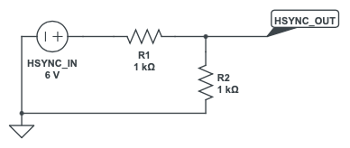
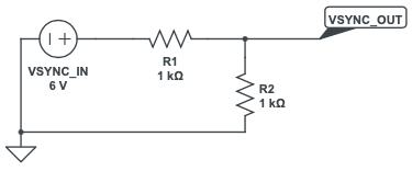
Consider the following logic levels for digital lows and highs:
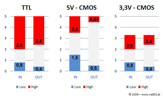
Since both signals are somewhat binary by default we just level them in for the FPGA.
For VSYNC_IN we see that signal goes low for sync (negative sync):

This is true for HSYNC_IN as well:

If we reconsider the video formats (Y3: 4.433618 MHz FM Version PAL, Y3 for NTSC is @3.579545 MHz) we get a better understanding of timings.
What we want to do is capture 8 bit for each pixel RRR GGG BB. If we use LVDS we have 8 iterations per pixel. This is somewhat a basic assumption for the what we call the pixel clock (a.k.a. the clock rate we need to run at in order to capture the distinct pixel values).
The HSYNC_IN freq is 15.6kHz divided by VSYNC_IN 50Hz giving us 313 lines per frame.
There is no color information when HSYNC_IN is low so we need to find out how long the high period is.
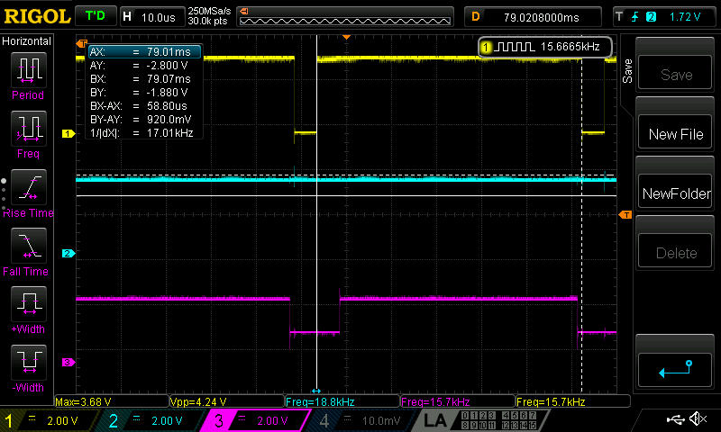
Period of HSYNC_IN (high) is 58.8us (yellow) and since we know that is 512 pixel values we need to define a proper clock frequency or capture frequency in order to get things right.
512 (pixels) x 8 iterations in 58.8 us = 69.65986395 MHz sample clock frequency.
With the 50MHz clock of the DE0 Nano we set a PLL with a 206 division and a 287 multiplier. This leads us close to the target frequency. We'll see if that is close enough.
Implementing simple row and column counters is easy: For each raising edge of HSYNC_IN we count one line. As soon as VSYNC_IN is low, we reset the counter.
As soon as HSYNC_IN is high we count every clock cycle. We chose the pixel clock to have 8 cycles for each of the 512 pixels , making our counter to count to 4096.
As we see in this picture, VSYNC_low cuts off 4 lines (based upon the criteria above) so the row counter ends with 310 (actually 309 because line 310 is cut off after 69ish pixels) (instead of the theoretical 313).
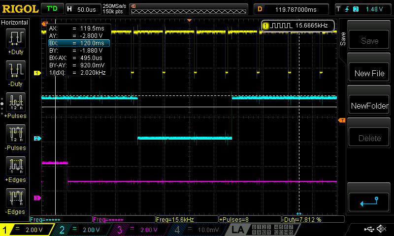
Right now it does not matter if we reset row count when VSYNC_IN is low or when it switches from low to high (or vice versa) since there is a huge front porch and still 2 lines back porch.
Last but not least we increment column count only when the last 3 bits are '111' (2^3 = 8) since we take 8 cycles per pixel to capture the color information.
At this point we should get somewhat accurate xy coordinates for the RAM:


It is as accurate as we can have it for now. Assuming the front and back porches, the data itself should be good enough.
At this point I think it is better to go down the process before capturing color values - I suppose there are some changes to this logic to come sooner or later.
We want to have a line buffer (RAM) where we can write a whole line. Afterwards we want to clock this line to SDRAM, which will act as some sort of frame buffer.
A separate VGA module should run on its own frequency domain and stream data to the VGA output.
Wiring up R, G & B
Being convinced the ADC is too slow and not having one with decent speed at hand (like: TVP5151) I decided to try something I read about the use of LVDS (Low Voltage Differential Signaling) input pairs.
I'd say at this point this is quite an ambitious project since it touches so many domains unknown to me but hey, one never stops learning. 👨🏻🏫
Bear with all the wrongs I do and write 😁
So what does an LVDS do? I'm giving a brief from this brilliant explanation (the best I found for beginners, kudos 🙇).
Traditional single ended signalling uses one wire where a voltage is applied. This voltage travels to a common ground. Multiple signals have one wire each, but can share a common ground wire.
Differential signalling does not use a ground wire, but uses two wires of opposite polarity. This means for a bit signal if the polarity between the two wires is positive we have a 1, if negative we have 0. Since both signals have the same amplitude but only opposite polarity the cancel each other out (ideally) and no current (ideally) flows. This reduces the need for a common ground (theoretically speaking). There are a lot advantages to LVDS over single ended signalling: since two lines have reverse polarity the create electromagnetic fields of equal magnitude but opposite polarity. This minimises electromagnetic interference (EMI). Another issue is signal to noise ratio (SNR). Single ended signals operate on relative high voltages (usually 3-5 V) whereas LVDS work a significant lower voltages.
That's theory 🧮
What we really want to do is comparing the voltage level of each color channel 8 times against a reference voltage in order to get the exact value. Comparators in this environment work far faster than the ADC.
For the three color channels we do nothing more than just put 75 Ohm pull-up resistors to each color signal.
The I/O
I've never been equipped with a second floppy drive, rom cartridge or an external hard drive - not mentioning fancy things like UltraSatan, CosmoEx, a happy drive or god knows what.
Since this whole restoration is some sort of winter game I decide to go down the FPGA path and interface to the ACSI interface.
...to be continued!
Useful Links
http://www.atarimuseum.de/1040st.htm - good summary of what that home computer is at the Atari Museum
https://www.atari-forum.com/viewtopic.php?t=23957
https://www.atari-forum.com/viewtopic.php?t=30813
http://www.clausbrod.de/cgi-bin/view.pl/Atari/WebHome
https://www.exxoshost.co.uk/atari/last/psu/index.htm
http://info-coach.fr/atari/hardware/FD-Hard.php
https://www.forum64.de/index.php?thread/3437-tos-chips-oder-welches-tos-hat-mein-rechner/
https://blog.troed.se/projects/atari-st-wakestate-nudger/
http://alive.atari.org/alive9/ovrscn1.php
https://www.exxoshost.co.uk/forum/viewtopic.php?f=29&t=296&start=30
http://www.harbaum.org/till/atari/multisync.html
https://info-coach.fr/atari/hardware/video.php#video_composite
https://www.exxoshost.co.uk/forum/viewtopic.php?t=94
https://www.atarimagazines.com/startv1n2/ProbingTheFDC.html
https://www.emuparadise.me/Atari_ST_ROMs/63
https://www.exxoshost.co.uk/forum/viewtopic.php?t=1448
https://sites.google.com/site/fpgaandco/de0-nano-analog-video
https://muckypaws.com/2021/01/27/greaseweazle-trouble-shooting1/
https://github.com/keirf/Greaseweazle/wiki/Troubleshooting-FAQ
https://intentionallogic.com/2018/01/23/adc-in-an-fpga-part-1/
https://www.atari-forum.com/viewtopic.php?t=25522
https://hackaday.io/project/5033-de0-nano-fpga-to-vga-output
http://ww1.microchip.com/downloads/en/DeviceDoc/AT91SAM_pll.htm
