MaaBC: Motorola MC68000 as a Breadboard Computer 🤦
"Just remember that a CPU is literally a rock that we tricked into thinking. Not to oversimplify: first you have to flatten the rock and put lightning inside it." - @daisyowl, 14.03.2017
Sooo... This has been on my list for so many years now: putting a M68k on a breadboard and let it actually do something. This whole thing has been inspired by the fact that I grew up with ATARI ❤️ and - having something for the underdog - the fact the Motorola 68000 architecture was superior over the Intel 8086. But that war has been lost to clever sales and marketing long ago.
I have been preparing for this on and off for quite some time. Thinking about the pros and cons of the setup, e.g. connecting some sort of Arduino thingy to mimic address and data registers along with some other external peripherals didn't feel good. But using a Logic Pattern Generator - in my case an HP 8170A - for memory simulation felt fantastic! 🤩
Unfortunately (i) the 8170A only goes up to a clocking of 2MHz. Unfortunately (ii) it is quite a stepping stone to connect a modern PC to GPIB - the versatile HP communication protocol. Anyways, let's care of that later on. Frist steps first:
Ticking away the moments that make up a dull day, or... the clock!
The actual CPU being the guinea pig is a MC68000-P12. Per data sheet it'll run from 4MHz to 12.5MHz. From that spec it makes sense to start somewhere rather low, as breadboards are not known for carrying high frequencies in cultivated manner. Brave enough let's go with a 6MHz oscillator. We could still implement a frequency divider using flip flops if necessary.
The crystal for setting up an oscillator happens to be a HC-49U with a fundamental frequency of 6MHz. But how do we get this to generate a clock? Turns out there are numerous circuits one can build for generating a clock signal from a crystal. Citing an internet source:
"Oscillator design is an imperfect art at best. Combinations of theoretical and experimental design techniques should be used."
I love getting some encouragement right at the beginning! After some research it turns out a Pierce Oscillator looks like it is the most simple design:
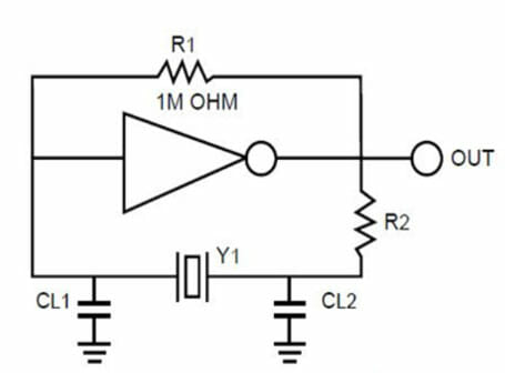
This circuit is super easy to setup. The load capacitance of the crystal is 20pF (see data sheet). In order to match this capacitance we need to get CL1 and CL2 correct. There is formula for that 🎉
C(load) = (CL1)(CL2)/(CL1 + CL2) + stray capacitance.
I found best results with a 20pF and a 10pF cap which - given the equation - is pretty far off the theoretical load capacitance. I assume there is quite some stray capacitance on the breadboard - but what do I know? 🤷♂️
R1 looks good at 1M Ohm and R2 seems to do the trick at 680 Ohm.
For the CMOS Inverter I took an ordinary cheapy cheap SN74HC14N which is a hex Schmitt Trigger inverter.
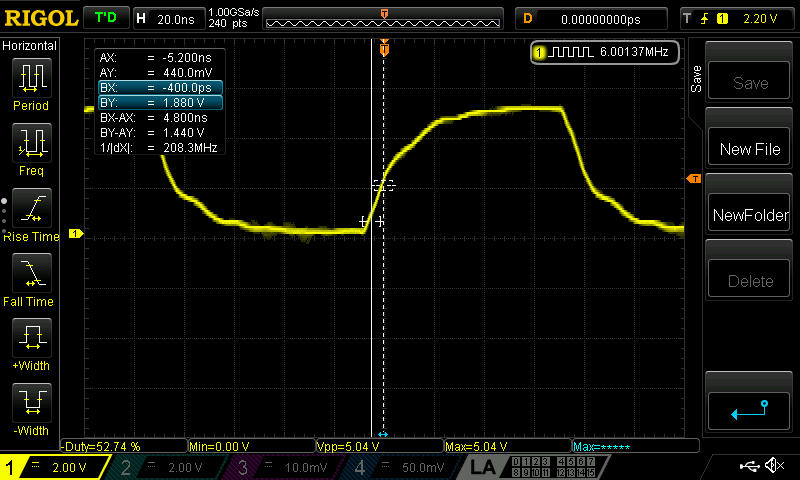
The output of the circuit has a range of -2.2V to +6.4V. That's out of spec for the M68k! A 500 Ohm resistor in series with the output dampens the signal to a range of 0V to +5.1V which is perfectly in range for the CPU.
The M86k data sheets states some requirements for the clock input:
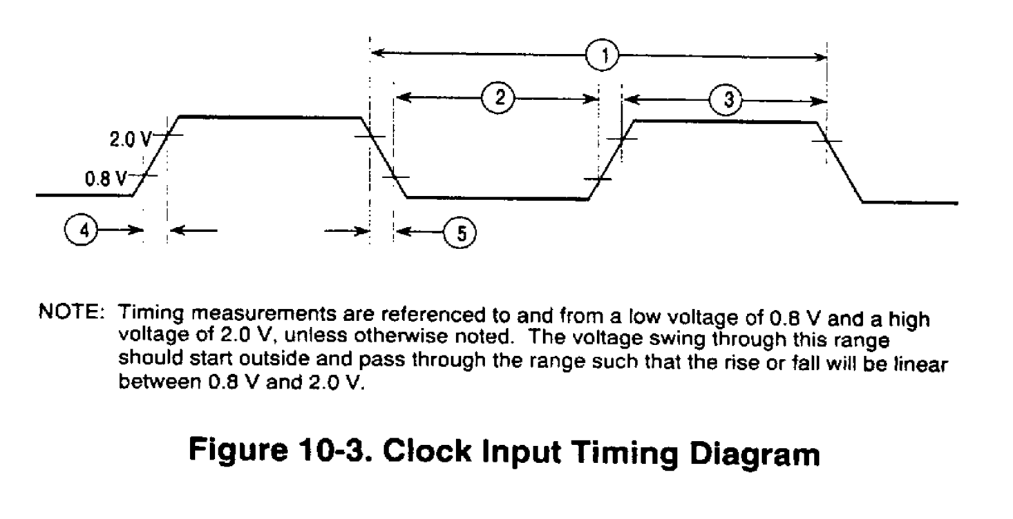
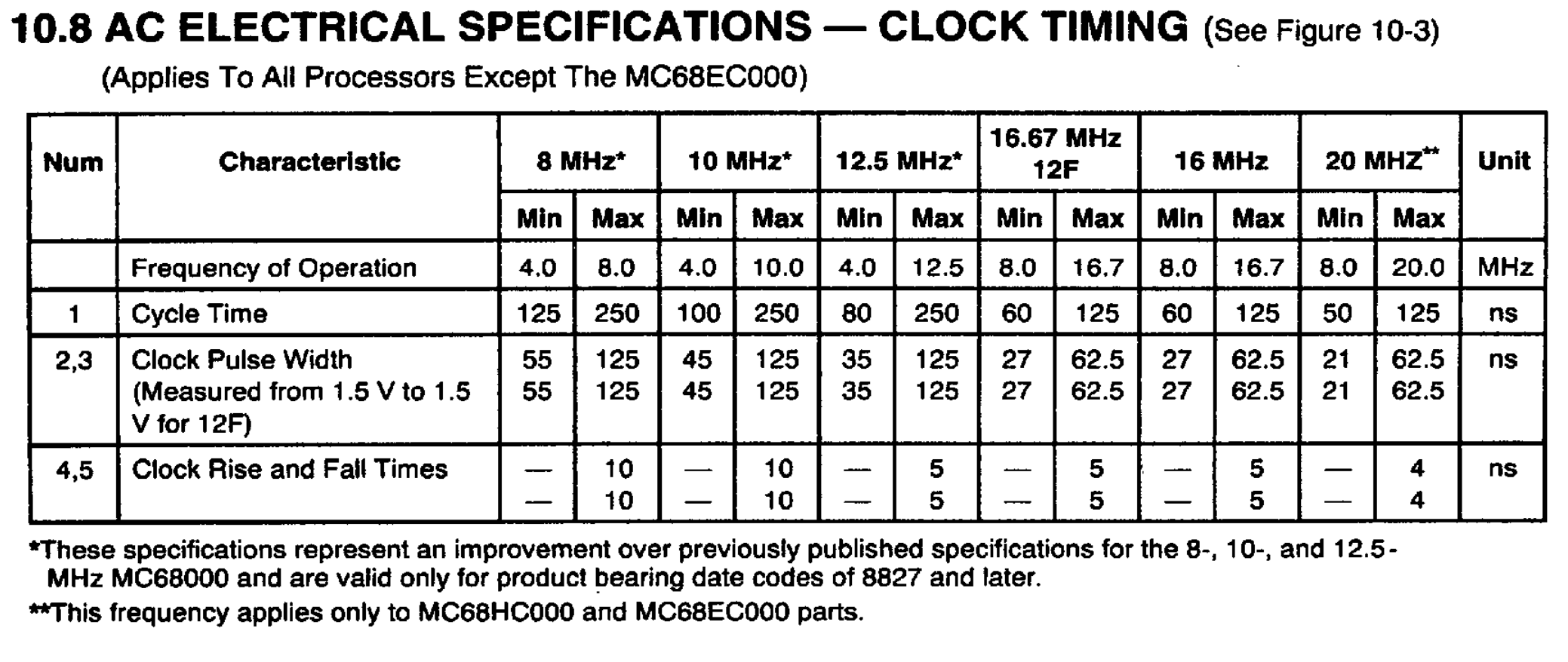
So we definitely want to get the clock rise and fall times right as well. For the rise times we get well below 5ns, the rise time is a good bit off. But we leave that for now and see how far we come.
This is the final clock generating circuit result:
Let's wire it up!
Googling the inter webs helps to get jump started here so let's consolidate what I've found. This is the pin out of the CPU for reference:
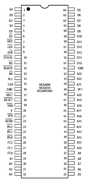
Obviously we want to tie Vcc and GND to +5V and ground accordingly. A no brainer I'd say! 🧠
Clock Input
Our fresh off the factory clock goes to CLK.
Datalines D0..D15
The M68k expects the datelines in a defined state. Given that we tie them to GND. Might be they need a pull-down/pull-up 🤷♂️
/DTACK (the famous Data Transfer Acknowledge)
This relict from old times should acknowledge it did set data on the databus. If not yet acknowledged, the CPU would go into a wait state until DTACK would be pulled low. We don't care about that for now so we tie it to GND already.
BERR
The Bus Error informs the CPU about an error with an MMU or such. Our system is very simple so we tie this to 5V.
/BR, /BG, /BGACK
Those pins control Direct Memory Access (DMA). This is complex enough so we don't care about it for now. We ignore BG completely and tie BR and BGACK to 5V.
/IPL0, /IPL1, /IPL2
Those pins handle interrupt control, which we do not have so we put them to 5V.
/VPA
This is one of the pins interfacing with 6800-series parts. We just tie it to 5V.
That's basically it! We just put some decoupling caps between +5V and GND for good reasons and we are ready for a test. Oh! Wait! There is one little detail missing: Just firing up the power won't start the CPU right away. It needs a Power-On Reset pulse once clock and power are there. The User Manual states:
For the initial reset, RESET and HALT must be asserted for at least 100 ms. For a subsequent external reset, asserting these signals for 10 clock cycles or longer resets the processor.
There are a couple of options:
- using a 555 timer to wait some milliseconds after power-up,
- using a Maxim DS1813,
- using two transistors which share a base which triggers both signals.
- triggering the reset manually with a push button.
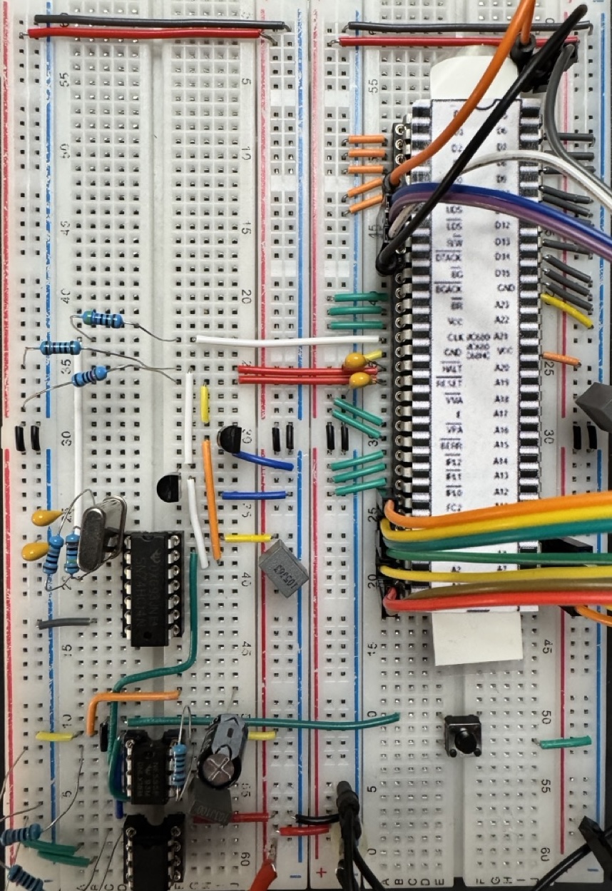
I went with two transistors in order to have both signals driven on the same timescale making readings on the instruments so much easier.
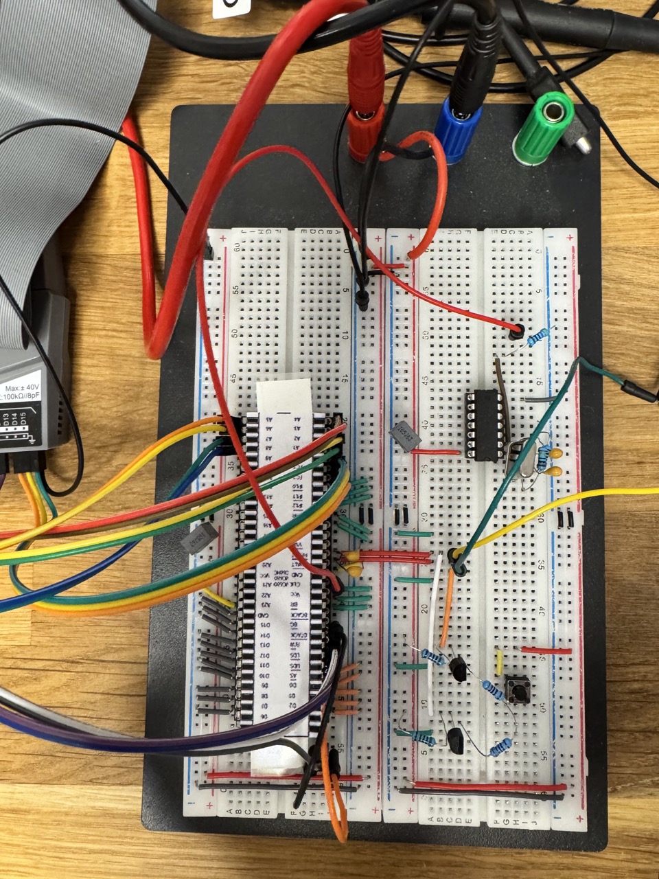
For convenience reasons I hooked the first 8 address bits to the logic analyser to see what happens. Nothing on Power-On - of course! We didn't trigger /RESET & /HALT yet. After pressing the button we see the CPU iterating the memory address space in all its glory:
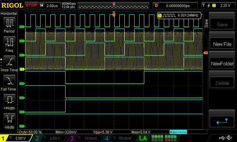
Actually, seeing this is quite rewarding! 😅 Also rewarding: the whole circuit draws approx. 202mA of current. Looks like all conditions are normal... 😀
But why is the CPU cycling through data address space? Let's dive into the startup sequence of the M68k with a new oscilloscope reading (CH1: CLK, CH2: /RESET & /HALT, CH3: /AS):
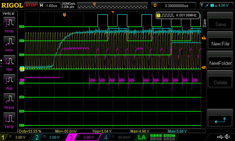
When /RESET & /HALT go high, approx. at the +2V mark, the CPU starts to carry out some action 🎥. We see at that point, /AS goes high for ˜12 clock cycles, going low afterwards. So what is /AS indicating? The M68000 User Manual states:
Address Strobe (AS)
This three-state signal indicates that the information on the address bus is a valid address.
Getting more details regarding READ operations from the M68k User Manual shows how reading data actually works. BUS MASTER refers to the CPU itself, SLAVE refers to a general memory controller:
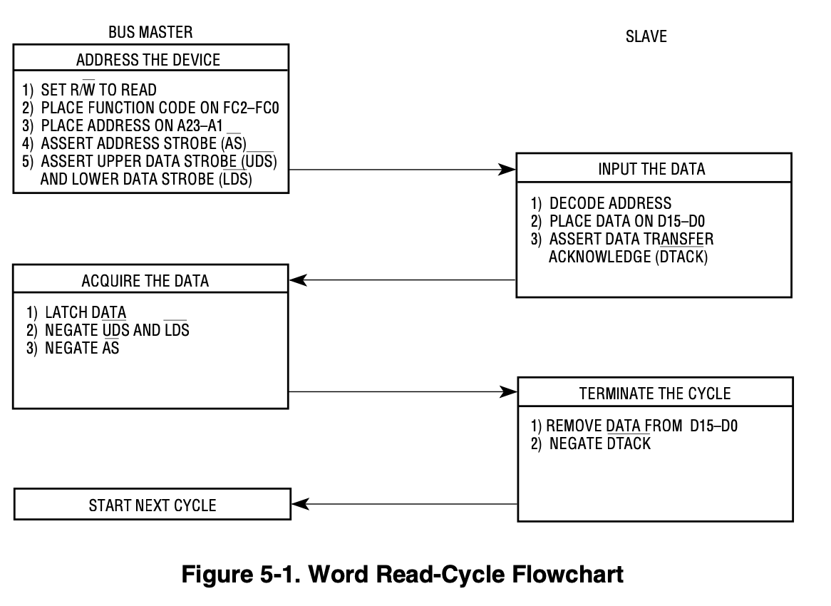
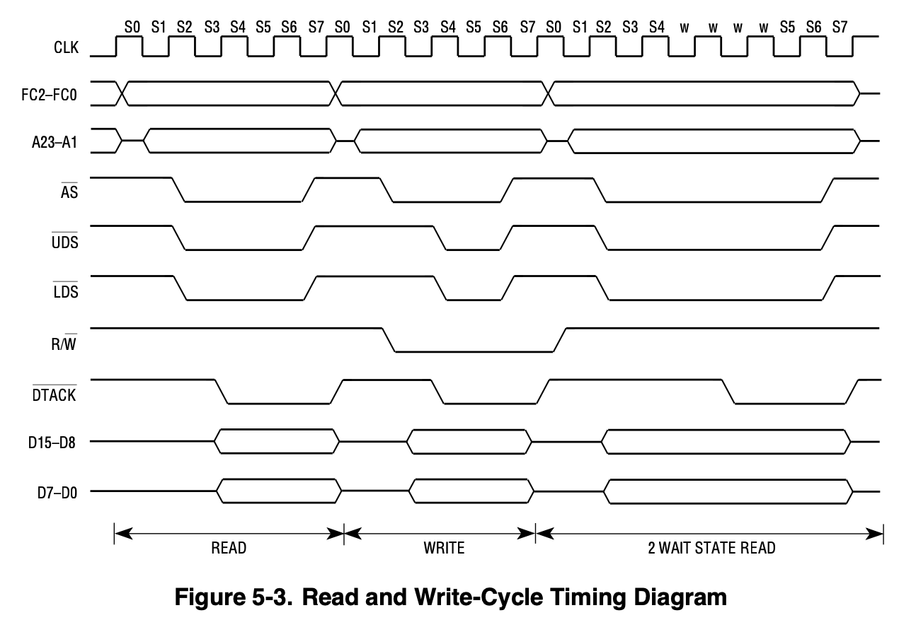
It also states:
When RESET and HALT are driven by an external device, the entire system, including the processor, is reset. Resetting the processor initializes the internal state. The processor reads the reset vector table entry (address $00000) and loads the contents into the supervisor stack pointer (SSP).
We actually do not care for the data at the address the CPU asks for but always return D15-D0 = 0. So in our case the CPU reads 0x0 for address 0x0, since we connected D15-D0 to GND.
Next, the processor loads the contents of address $00004 (vector table entry 1) into the program counter. Then the processor initializes the interrupt level in the status register to a value of seven.
Since it is reading two words (2x32 bits), it reads address 0x0, 0x1, 0x2 and 0x3.
Per other documentation:
When the MC68000 powers up or receives a reset signal, it fetches two 32-bit values (Key Data Sizes in the MC68000 are: Byte - 8 bits, Word - 16 bits, Long Word - 32 bits) from specific memory addresses, known as the reset vector:
- The Initial Stack Pointer (ISP) from address 0x00000000 to 0x00000001 first. The processor loads this value into the A7 (stack pointer) register. It will be used as the initial location for the system stack.
- The Initial Program Counter (PC) from address: 0x00000002 to 0x00000003. The processor loads this value into the Program Counter (PC). This is the address of the first instruction to execute after reset.
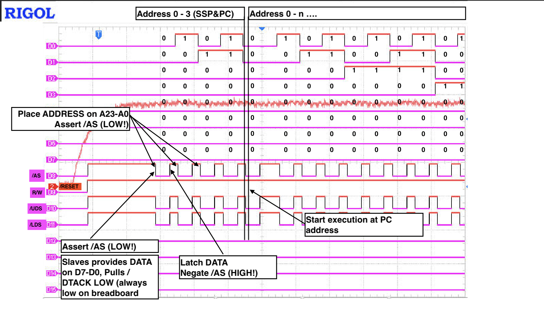
And this is what we are seeing. It took me quite some time to understand why the logic analyser output shows the memory location count in steps of +1 as per the documentation we learn it only talks in even memory addresses... 🤔 I would have expected it to check address 0x0, 0x2, ... . The answer is: The M68k doesn't care about the memory controlling part. It assumes when putting an address on the address bus the controller knows:
- are we doing a word read (UDS and LDS low) or
- are we reading a byte from memory, in which case UDS or LDS is high indicating the MSB or LSB.
Given that one memory address from the view of the CPU holds two bytes our hypothetical memory controller needs to align the address in its memory table a slight bit. If we expect to have an 8 bit storage IC, let's say in eprom, we need to double the address bus value to find the exact location in memory. Now binary-wise, doubling is pretty easy: it is just a shift left! 👈
However one little concern remains: When writing code for the M68k, does the compiler take care of the memory alignment, since - code-wise - we always make sure we talk even memory addresses - to be investigated! 👮
Given we only have 23 address lines each one holding two (!) bytes of memory, we now know why the M86k can access up to 16MB of memory, which is pretty cool.
Now, everything we see seems to make great sense!
The value in the PC register points to the memory location of the first instruction. The processor begins fetching and executing instructions from this address. Typically, the first instructions initialize critical hardware components, set up memory, and prepare the system for operation. Our very basic system won't do that 😬
After reset, the MC68000 starts in Supervisor Mode with interrupts disabled, which is a privileged operating mode. The Supervisor Stack Pointer (SSP) is used, which is initialized from the reset vector (ISP). User Mode is not enabled until explicitly set by software.
Since our system RAM always returns 0x0, the CPU starts program execution at 0x0. As the DATA bus always returns 0x0, which equals instruction ORI.B #0,D0, the program counter is incremented by one and that memory address is read. What's actually happening is that the CPU executes ORI.B #0,D0, jumps to the next memory address, reads the same instruction again and so on and so forth, cycling through memory forever and ever. This is supposed to be called the 'freerun mode'.
But in order to properly start execution we should build something which asserts HALT and RESET after power on automatically without the need for human intervention.
I use a Voltage Comparator (LM393) which pulls /HALT and /RESET high as soon as the supply voltage is well beyond a certain voltage level. In order to set Vref for the comparator to an appropriate value, I use a standard voltage divider with two resistors. Since we have quite some ringing on the breadboard around 3.5V looks pretty stable. Going above that, e.g. with only R1=2K brings Vref and Vcc too close and produces major fluctuations at the output of the comparator. For reference a brief 101 on comparators:
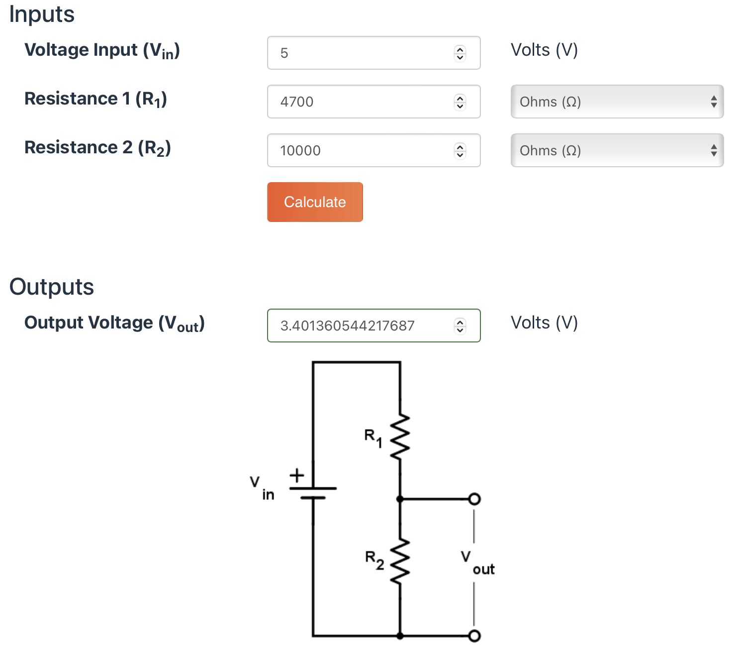
Given the circumstance, this setup is pretty reliable. As soon as Vcc comes up, the M68k starts doing its job right away 💪 Even pressing the manual reset asserts HALT and RESET and the CPU starts all over again. Examining the manual there is this statement:
For the initial reset, RESET and HALT must be asserted for at least 100 ms. For a subsequent external reset, asserting these signals for 10 clock cycles or longer resets the processor. However, an external reset signal that is asserted while the processor is executing a reset instruction is ignored. Since the processor asserts the RESET signal for 124 clock cycles during execution of a reset instruction, an external reset should assert RESET for at least 132 clock periods.
For the first interval, we are not quite there. We assert HALT&RESET basically as soon as the voltage is sufficient for our pierce oscillator reaching a stable oscillation and having enough power on Vcc. We need a component which produces at least 100ms delay. Iiiii'd say it's time to get a 555 timer from the drawer 😁👍
For the second time interval, we just need to make sure we press our reset button longer than 132 clock cycles. Our CLK is 6MHz so 132 cycles are approx 0,000022 seconds. On a human scale I assume we can't be quicker.
Let's combine it with a single circuit: As soon as Vcc reaches a sufficient level, the 555 is triggered and and pulls its output high for the capacitor-resistor-definded period. We put this signal into the hex inverter (up to now we only used one inverter out of six) and invert the signal. The inverted signal switches a PNP () transistor which pulls HALT and RESET to low for that period of time. This covers the power-on timing. For manual reset, a switch is connected to the 555 trigger pin. When the switch is pressed, the timer (and the subsequent inverter and transistor) pull HALT&RESET low for the configured period at the 555. Since HALT and RESET are open collectors, each of them has its own PNP transistor connected in order to separate the lines whenever the CPU itself pulls one of the two pins low. Up to now, our setup looks like this:
The values chosen for the 555 timer are t = 1.1 x R1 x C1.
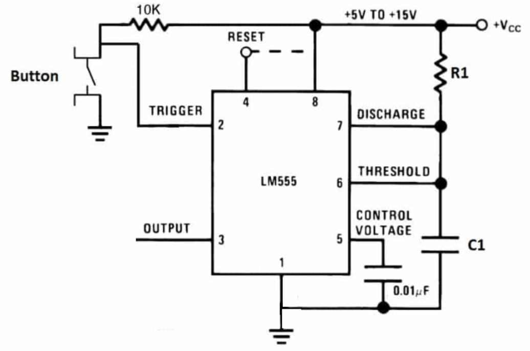
For this setup it is t = 1.1 x 10,000.00 O x 0.00001 F = 0.11 = 1.1 seconds. That's far more than necessary but we could fine tune that any time by changing R and C.
A couple of tests show this is quite a nice setup! 🥳
At this point we should be able design a memory controller allowing read and write operations and write a simple program which executes an operation and jumps back to the initial program counter location. It is veeeery tempting to dive into the next rabbit hole which is the MC68451 Memory Management Unit (MMU) designed for the M68k. Just reading the documentation creates this tickling feeling 😬
We could go down several paths: using some 74HC245 to handle data transfer / latch address and data between memory and the CPU or using those IC with some level converters to connect to an ESP32 interface or we even could try to connect some EEPROMS directly.
About EEPROMS: Consider using them as read/write memory is not too bad. However I'd say it is not their main purpose. Maybe FRAM is a better alternative. We'll see...
I guess best way is to wire two EEPROMS directly to the address and data bus in order to see how that goes. A second connection will be through a Teensy 4.1 and some level shifters in order to interact with the CPU without having the need to constantly manually erase and write an EEPROM.
Teensy it is...
Let's use a Teensy to connect the M68k! Since it does not have enough pins for address bus, data bus, various status pins etc. I guess we need to reduce the data and address pins a bit at least. That's quite easy using SIPO (serial in / parallel out) and PISO (parallel in / serial out - you guessed it!) ICs. We lose a couple of clock cycles but since we do not want to work on the edge of max performance this will be ok.
A1 to A23 of the address bus go in strands of 8 each to three 74HC165 parallel to serial converters. As soon as AS goes low, this will trigger an interrupt in the Teensy, quickly reading in the adress bus pins.
Since the data bus is actually tri-state there will a but more to this connection. Basically we connect the 16 data bus pins (D0 to D15) in groups of 8 to two 74HC245 - which are 8 bit tri-state transceivers. Those can be set to work as input or output (through the according DIR pin) and can be disabled completely making the connection to the M68k data bus floating.
We need to consider two modes from the point of the view of the Teensy: Writing data to the transceivers or reading data from the transceivers. For writing to the transceivers we use two 75HC595 (serial to parallel converters). The Teensy writes serial data to the 74HC595, once done latches and enabled their output, which pass the data to the transceivers.
Since we are working in the CMOS world we need some level shifters between all the ICs and the Teensy. This is done with HW-221 out-of-the-box level shifters.
... and a bit of logic
Finally we need to consider affirming DTACK low when the data is put on the data bus and ready to be read. Code wise this is easy but the timing gets messy here so we just OR the /AS signal from M68k and the /DTACK from the Teensy. When the M68k sets AS the OR takes care that DTACK is low so we do not get into trouble and the timing on the Teensy side doesn't matter too much. We have plenty of time putting it high again.
http://electromotiveforces.blogspot.com/2011/09/checking-out-pierce-oscillator.html
http://jefftranter.blogspot.com/2016/11/building-68000-single-board-computer_30.html
https://www.allaboutcircuits.com/tools/voltage-divider-calculator/
https://www.circuitbasics.com/555-timer-basics-monostable-mode/
https://www.electronics-tutorials.ws/opamp/op-amp-comparator.html